USB-programmable Cortex-M4
The USB-programmable Core.ST.L4.1 (formerly Core.U.1) is based on the 80-MHz 32-bit Cortex-M4 STM32L422 with 128KB flash, 40KB SRAM, and a CoreMark score of 273.55. The exposed pads provide a user-configurable combination of two fast-mode-plus I2C ports, one SPI port, three 12-bit ADCs, multiple timers, USART, an onboard comparator, and capacitive-touch input. A programmable onboard LED provides a convenient status indicator. If more I/O is needed, consider the larger Core.ST.L4.2 in a T48-22 package.
Product Info
- Status
- Beta
- In Stock
- Yes
- Pricing
Qty Each 1+ 15.00 $ 10+ 13.50 $ 50+ 12.75 $
Technical Summary
Resources & Links
- Datasheet
- Download PDF
- JSON Tile Definition
- v0.34 (Jun 2, 2026)
- Drivers
- Documentation|GitHub
- Discussion
- Discord
Onboard Features
- Status LEDRed · PA8 · (active-high)
- Clock16 MHz HSI16 · 4 MHz MSI · 48 MHz HSI48 — boots HSI16
Configuration
- GPIO pad configuration
- EXTIPullSpeedDirectionOutput default
- Pad function assignments
- 9 pads · see Pad Assignments
- Clock configuration
- Low (8MHz, MSI)Medium (16MHz, MSI)High (48MHz, MSI)Max (80MHz, HSI16 + PLL)
- Programming methods
- USB DFUUSART1USART2USART3I²C1I²C3SPI1
- Interfaces
- USBI²C1I²C3SPI1USART1
Enable / role / speed configurable per interface.
Application Notes
Bootloading
When the chip is blank, it will default into the bootloader when connected over USB. Once there is code in the program space, you need to hold the BOOT0 pin low during reset (either power-on or via the NRST pin) to enter the bootloader.
LED
The onboard LED is connected to PA8 in an active-high configuration.
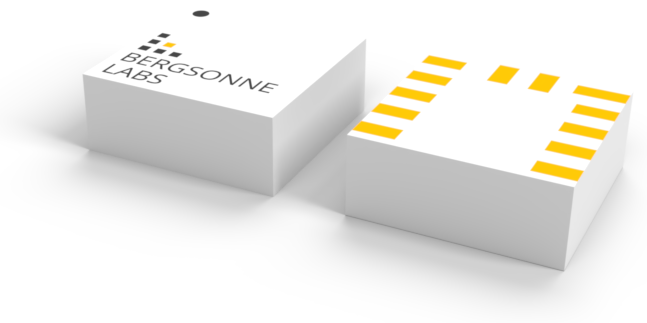
Pad Assignments
| Pad | ⏻ | D | A | ○ | ||
|---|---|---|---|---|---|---|
| 1 | GND | · | · | · | · | · |
| 2 | · | A7, I2C3.CLK, SPI1.MOSI | 12 | 1.1N | · | · |
| 3 | · | A1, I2C1.SMBA, SPI1.CLK | 6 | 2.2, 15.1N | · | COMP1.+ |
| 4 | · | B6, I2C1.CLK, USART1.TX | · | 16.1N, LP1.ETR | · | G2.IO3 |
| 5 | · | B7, I2C1.DAT, USART1.RX | · | LP1.2 | · | G2.IO4 |
| 6 | · | A12, SPI1.MOSI, USART1.RTS_DE, USB.DP | · | 1.ETR | · | · |
| 7 | · | A11, SPI1.MISO, USART1.CTS, USB.DM | · | 1.4, 1.BKIN2, 1.BKIN2_COMP1 | · | COMP1.OUT |
| 8 | · | B4, I2C3.DAT, SPI1.MISO, USART1.CTS | · | · | · | G2.IO1 |
| 9 | · | A4, SPI1.CS | · | LP2.OUT | · | COMP1.- |
| 10 | V+ | · | · | · | · | · |
| 11 | · | H3 | · | · | BOOT0 | · |
| 12 | · | · | · | · | NRST | · |
USB
USB- Mode
- Max Clock
- —
- Address
- —
- Format
- —
| Function | Required | Pad(s) |
|---|---|---|
| USB.DP | Yes | 6 |
| USB.DM | Yes | 7 |
I2C1
I2C- Mode
- master, slave
- Max Clock
- 1MHz
- Address
- programmable
- Format
- 7-bit address
| Function | Required | Pad(s) |
|---|---|---|
| I2C1.CLK | Yes | 4 |
| I2C1.DAT | Yes | 5 |
| I2C1.SMBA | No | 3 |
I2C3
I2C- Mode
- master, slave
- Max Clock
- 1MHz
- Address
- programmable
- Format
- 7-bit address
| Function | Required | Pad(s) |
|---|---|---|
| I2C3.CLK | Yes | 2 |
| I2C3.DAT | Yes | 8 |
SPI1
SPI- Mode
- master, slave
- Max Clock
- 40Mhz (master), 20MHz (slave)
- Address
- —
- Format
- —
| Function | Required | Pad(s) |
|---|---|---|
| SPI1.CLK | Yes | 3 |
| SPI1.MISO | No | 7, 8 |
| SPI1.CS | No | 9 |
| SPI1.MOSI | No | 2, 6 |
USART1
USART- Mode
- Max Clock
- —
- Address
- —
- Format
- —
| Function | Required | Pad(s) |
|---|---|---|
| USART1.TX | Yes | 4 |
| USART1.RX | Yes | 5 |
| USART1.RTS_DE | No | 6 |
| USART1.CTS | No | 7, 8 |
Development Product — This is an electronic development module intended for evaluation, prototyping, and integration into other designs by qualified engineers and developers. It is not a finished consumer product and has not been independently certified for FCC, CE, UL, or other regulatory compliance. The integrator of this module into a finished product is responsible for obtaining all necessary certifications. Not intended for use in life-support systems, safety-critical applications, or any application where failure could result in personal injury or property damage. See our Terms of Sale for full details.